The advantages of laser ball planting technology in BGA chip packaging process
A chip is an electronic component manufactured by microelectronics technology that integrates circuits and systems onto a tiny silicon wafer. It is an important component of modern technology, ubiquitous and affecting people's production and life. The continuous expansion and innovation of the types, manufacturing processes, and application fields of chips are of great significance for the development of modern information society and the progress of human society.

What is BGA?
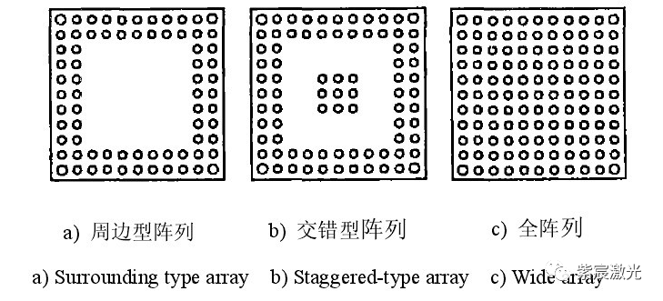
The full name of BGA is Ball Grid Array (PCB), which is a packaging method for integrated circuits using organic carriers. Used for permanent installation of microprocessors and other devices. BGA can provide more interconnect connections than dual inline or flat packaging. You can use the entire bottom of the device, not just the periphery. Connect the encapsulated leads to the core, and the routing of the encapsulated wires or solder balls is on average shorter than that of the surrounding types, resulting in better performance at high speeds. Its characteristics include:
① Reduced packaging area;
② Increased functionality and increased number of pins;
③ PCB board can self center and easily solder during solution soldering;
④ High reliability;
⑤ Good electrical performance and low overall cost.
PCB boards with BGA generally have more small holes, and most customers design through holes under BGA with a finished hole diameter of 8-12mil. The distance from the surface of BGA to the hole is generally not less than 10.5mil, taking the specification of 31.5mil as an example. The BGA through-hole needs to be plugged, and the BGA pad does not allow ink to be applied. No drilling is allowed on the BGA pad.

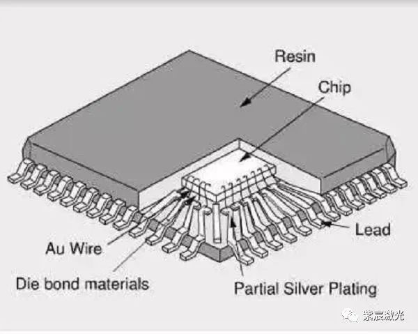
At present, many chip packages are BGA type, and the biggest advantage of this type of packaging is that it can save space on the board. The most common is the upward structure of the chip, and a downward structure is usually used for high heat treatment requirements. Most packages use chip bonding technology to connect chips to substrates and achieve electrical connections between chips and substrates. The same goes for BGA, but it mostly uses inverted chip interconnection technology. The use of inverted chip design can directly connect the heat sink to the chip, achieving better heat dissipation.
Packaging process flow
Preparation of wafer protrusions → wafer cutting → chip flip and reflow soldering → bottom filling → distribution of thermal grease and sealing solder → capping → assembly of solder balls → reflow soldering → marking → separation final inspection → testing → packaging.
Inverted soldering overcomes the problem of the center to center distance limit of wire bonding pads and provides more convenience in the design of power/ground distribution of chips, providing a more complete signal for high-frequency and high-power devices. The soldering of BGA devices requires precise control, usually completed through automated processes, such as computer-controlled automatic laser ball planting and reflow soldering furnaces.
In the field of high-density chip wafer packaging technology, when making bumps on the wafer, the subsequent packaging of micro solder joints on the wafer is mainly achieved using ultra-fine spacing and high-density bump arrays. This is an important link in high-density chip wafer packaging, which requires high requirements for process effectiveness, operation, and cost.
At present, there are three main ways to obtain protrusions: electroplating, printing solder paste curing, and ball planting. However, the electroplating method has disadvantages such as complex process and high cost, long manufacturing cycle, and environmental pollution, while the printing solder paste method is not easy to control the height of protrusions, making it difficult to produce less than 200 μ The convex point of m. The advantages of laser ball planting are even more prominent: due to the lack of flux inside the solder balls, laser heating and melting will not cause splashing, and after solidification, it will be full and smooth, without any additional processes such as subsequent cleaning or surface treatment for the solder pads. Meanwhile, due to the constant amount of tin, ball splitting welding has the advantages of fast speed and high accuracy, and has been increasingly applied in the field of BGA chip ball planting.
Advantages of laser ball planting technology
The 01 system uses fiber laser as the planting ball heat source, with high electro-optical conversion efficiency and stable energy;
02 is compatible with commonly used materials such as Sn Ag Cu, Sn Bi Ag, etc. with specifications ranging from 0.07mm to 0.2mm, to meet the process requirements of different fields. At the same time, it is equipped with CCD camera positioning to ensure the accuracy of planting balls;
03 non-contact tin spraying and planting method, with a planting speed of 3-5 points/s, stable and consistent tin content at convex points, simple process, and easy implementation of production automation,
The 04 process does not require overall heating, and the thermal impact during the ball planting process is small, which has no effect on the material of the wafer around the pre planted protrusions;
05 tin material does not contain any flux components, eliminating the need for post weld cleaning. The laser melting and tin spraying process in the laser planting ball can achieve zero pollution production, which is more in line with the concept of green manufacturing.