This article summarizes the definition, function, circuit analysis, and design points of pre bias transistors, emphasizing their advantages in reducing PCB size and reducing component count, and reminding them to make reasonable choices to match microcontrollers and loads.
What is a pre biased transistor?
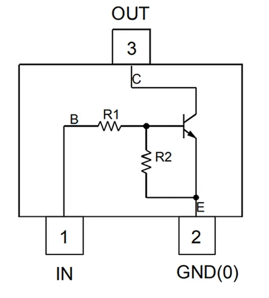
A pre biased transistor is a transistor that integrates a bias resistor during the manufacturing process. This design is cost-effective, as the integrated components save on the cost of printed circuit boards (PCBs) and reduce the number of items in the bill of materials (BOM). A typical product is the DDTD113ZC-7-F NPN transistor from Dior, packaged in SOT-23-3, as shown in Figure 1. This pre biased transistor includes a 1 kiloohm series current limiting resistor and a 10 kiloohm turn off resistor connected in parallel with the base emitter junction.

Figure 1: DDTD113ZC-7-F: Pre biased transistor with series resistor R1 and base to emitter resistor R2
How to use pre biased transistors in circuits?
Pre biased transistors are designed to be directly connected to digital logic such as microcontrollers, eliminating the need for additional auxiliary resistors. This can achieve a compact PCB design and reduce the number of components, as three traditional components are integrated into a single package.
What is the function of each resistor in a pre biased transistor?
A typical pre biased transistor consists of two internal resistors. They can be classified by function as follows:
Series current limiting resistor: Similar to the series resistor in LED circuits, this series resistor is used to limit the base current.
Turn off (shunt) resistor: This resistor connected in parallel with the base emitter junction of the transistor helps to turn off the transistor. When the input series resistor is disconnected, such as when the microcontroller I/O is set to high impedance or in ultra-low power consumption (ULP) mode at startup, it provides a leakage path to keep the base at zero volts. This turn off resistor also helps to reduce the leakage current between the ICE (collector emitter).
There are various pre biased NPN and PNP transistors available in the market for selection. Designers can choose products with the most suitable series resistance and turn off resistance to match their application requirements.
Essential Crystal Management Theory for Forced β Operation in Digital (Switching) Circuits
One of the characteristics of a transistor is its DC current gain (β), which is defined as the ratio of collector current to base current. For transistors operating in their linear region, this is an important indicator in analog design.
Linear operation should be avoided in digital (switch) design. Instead, we will focus on mandatory beta. Through this design technique, we intentionally over drive the transistor to ensure complete saturation, thereby deliberately avoiding the linear region. As a preliminary estimate, we assume a forced β of 10, but it should be noted that the forced β is significantly lower than the linear β.
Circuit analysis of pre biased transistor circuit
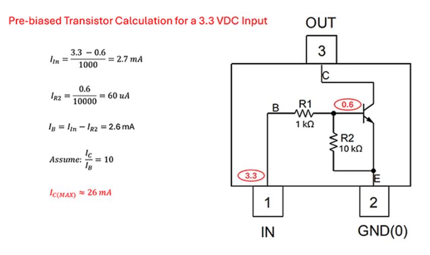
Figure 2 shows the circuit analysis of Dior DDTD113ZC-7-F. The R1 value of this transistor is 1 kiloohm, the R2 value is 10 kiloohms, and it has high gain.
In this application, the transistor is driven by a 3.3V DC logic signal:
The R1 series resistor limits the input current to 2.7 milliamps. This is a relatively low driving level that most microcontrollers can easily provide. However, as discussed in the next technical tip, this value may still be too high.
Turning off the resistor consumes a small portion of the input current. Depending on the ratio of R1 to R2 of the selected pre bias transistor, this may or may not be important for circuit calculations.
The base current is calculated as the input current minus the turn off resistor current.
Assuming a forced β condition, the maximum collector current is calculated as ten times the base current. Please note that this is a conservative estimate used to ensure that the transistor enters saturation state. You can improve this situation by testing extreme scenarios in the design.

Figure 2: Circuit analysis of Dior DDTD113ZC-7-F driven by 3.3V DC logic
Technical Tips:
A typical microcontroller has two current specifications, including the specification of each pin and the sum of all pin currents. For example, Renesas' R7FA4M1AB3CFM # AA0 is used for the latest Arduino UNO R4 development board. Most ports are capable of absorbing and outputting a current of 4 milliamps, while a few pins can withstand a current of 20 milliamps, but the total current limit for all output pins is 60 milliamps. Therefore, careful circuit analysis is required to ensure that the product's limitations are not exceeded.
Please note that the DDTD113ZC-7-F pre biased transistor from Dior displayed here was chosen due to its low R1 resistance value. For low current microcontrollers, transistors with higher input resistance may be a better match.
It is essential to evaluate each case (load) individually.
How fast is the speed of pre biased transistors?
The turn-on and turn off speed of transistors is determined by factors such as load characteristics, Miller capacitance, and saturation depth. The following are some design considerations directly related to the brief description of this project:
Transistors with deep saturation will turn off very slowly. By definition, forcing β bias will cause transistor depth saturation to avoid linear regions. This is an important consideration as the transistor will not turn off until the carriers are removed from its silicon structure.
The base current depends on the I/O voltage of the microcontroller and the R1/R2 ratio of the pre biased transistor. The saturation depth also depends on the load. For example, when the load approaches the limit of 26 milliamps, the speed of the circuit shown is faster than when lightly loaded with 5 milliamps. In other words, it is important to carefully select pre biased transistors to match the load and avoid over saturation.
The direct connection with the microcontroller eliminates the possibility of applying negative pulses to increase the turn off speed. In addition, due to the lack of exposed base connections, acceleration circuits such as Baker clamp cannot be implemented.
Overall, these design limitations indicate that pre biased transistors operate at moderate speeds. However, there are many different load and level conversion applications that can benefit from pre biased transistors. In all cases, designers should choose the most suitable pre bias transistor to achieve optimal matching between the microcontroller and the load.
Technical Tips:
Please remember that the traditional matching process is accomplished by selecting the appropriate resistor. Now, designers must choose pre biased transistors with internal resistors suitable for the task at hand. For example, transistors with R1 of 4.7 kiloohms or even 10 kiloohms may be more suitable for your design.
finally
Pre biased transistors are a convenient method to reduce PCB size and decrease the total number of components used in the design. It is essential to match the microcontroller with the load by selecting pre biased transistors with appropriate internal resistance.