Where is the position of the PCB? Almost all electronic devices have PCBs. They come in shades of green, red, blue, or black. A computer motherboard is a perfect example of a PCB. They exist in everyday appliances such as printers, digital clocks, televisions, microwave ovens, and even some simple items such as light switches.
If there is no reliable PCB, our society will run on PCBs, and households and businesses will not be able to operate smoothly now. In fact, commercial buildings typically accommodate more PCBs than the number of employees inside. Therefore, let's find out what PCB is and provide more insights.

PCB assembly method
The PCB assembly method includes the method of creating finished board assembly worksheets and blank board assembly worksheets using Excel programs stored in well-known computers, as well as the usage of the aforementioned worksheets; The finished board splicing worksheet is used to complete the process of splicing finished boards in the same or different phases on the blank board. Each column cell of the finished board splicing worksheet is used to place data of the same category for different blank board splicing schemes or the Excel internal function calculation formula for that data. Each row cell is used to place data of different categories for the same splicing scheme or the Excel internal function calculation formula for that data. The specific method for creating a finished board splicing worksheet is as follows:
(1) Start the Excel program stored in a well-known computer, create a new workbook, and select a worksheet;
(2) Enter the name of the worksheet using a cell in the table:
(3) Use a row of cells in the table as the header of the worksheet, and enter the category name of the data in each cell's column;
(4) Create data input area:
(5) Create data operation area
(6) Create data output area
(7) Create a panel calculation area
(8) Create an indirect output area using Excel's internal search and reference functions, referencing all data in the panel operation area worksheet, and placing it in the indirect output area.
PCB assembly techniques
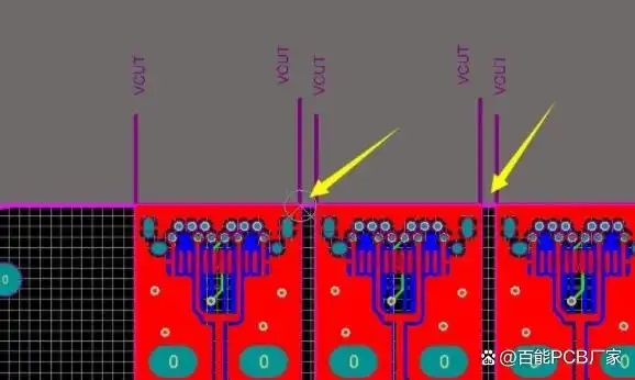
PCB splicing is a common task for PCB factories. What should be noted when splicing? What are the requirements for PCB assembly? To summarize for you:
Firstly, there is the issue of panel assembly. We know that the main problem with panel assembly is to save production costs. For PCB panel width ≤ 260mm~300mm, it varies depending on the production line. Because we may have a lot of materials and each material gun corresponds to one module in our processing equipment, if the splicing exceeds the range of the module, the processing speed will become very slow.
The outer frame (clamping edge) of the PCB panel should be carefully considered to ensure that the PCB panel will not deform after being fixed on the fixture (generally, V-grooves are not allowed on this edge). For the arrangement of components, the orientation of all components should be consistent, and there should be no mirroring, which can cause coordinate positioning problems during processing.
Secondly, there should be no connectors protruding from the edges (between the outer frame of the panel and the inner small board, or between small boards), as this would hinder the tool from separating the boards after welding is completed.
In order to ensure the position and levelness of the detection board, we need to set three or more positioning points at the edge of the board. By optically detecting these three points, we can obtain the reference coordinates of the entire processing and the levelness of the board.
The correct approach is to have a distance of 5mm from the edge and different distances when traveling in different directions (to distinguish the direction of entry): When setting the reference positioning point, usually leave a 1.5 mm larger unobstructed soldering area around the positioning point, and there should be no similar solder pads or other similar ones.
There should be at least three positioning holes on each small board, with a diameter of 3 ≤ 6 mm. Wiring or mounting is not allowed within 1mm of the edge positioning hole (to prevent misjudgment). PCB splicing is mainly used to save production and processing costs (which can make machine processing speed several times faster). Unreasonable design can lead to problems in the later stage. You can take a careful look to prevent problems.
Firstly, there is the issue of panel assembly. We know that the main problem with panel assembly is to save production costs. For PCB panel width ≤ 260mm~300mm, it varies depending on the production line. Because we may have a lot of materials and each material gun corresponds to one module in our processing equipment, if the splicing exceeds the range of the module, the processing speed will become very slow.