Advanced printed circuit boards (PCBs) are so complex that OEMs (original equipment manufacturers) often scratch their heads and doubt if their PCB assembly is going the right way. Specific circuit board applications face many challenges, but not all assembly plants have the ability to handle a critical area, which is radio frequency (RF) PCBs.
When the RF circuit operates at high frequencies above 50GHz, every additional metal on the circuit board will affect the impedance of the strictly controlled wiring. This may affect return loss and reflection, and may also lead to other signal integrity issues.
This becomes even more critical when the PCB is made of standard FR-4 or FR-6 PCB materials instead of more expensive RF compliant materials such as polytetrafluoroethylene (PTFE) or Astra MT77.
In addition, grounding holes are also crucial for RF PCBA. The final acceptance criteria for large grounding pads under QFN components specified in IPC-A-610 shall be agreed upon by the OEM and contract manufacturer (CM). IPC does stipulate that a 30% void on collapsed BGA solder balls is acceptable when the amount of solder is much less.
For OEMs producing RF PCB designs, their goal in this regard can be to achieve a void ratio of less than 25% (or even less than 10% in some cases) on large ground pads under QFN type components. Only by using the correct assembly procedure can the void rate be lower than 25% or 10%.
In addition to grounding holes, the five key PCB assembly aspects that OEMs need to closely monitor are component selection, PCB material selection, template design, reflow curve, and functional testing.
Component selection
When selecting components, not only should signal integrity requirements be considered, but also close attention should be paid to assembly requirements. Design engineers must understand the assembly challenges when choosing packaging. If lower difficulty packaging can be used to achieve the final result, then design engineers must choose these packaging.
Examples of active component packaging can be flip chip and micro BGA or QFN type packaging, while passive components can be 0201 size passive components rather than 01005 size passive components, especially capacitors. The challenges related to these components will be further discussed in the following text.
PCB material selection
PCB materials and surface treatment play a crucial role in the final wiring impedance. PCB companies are unable to use FR-4, PTFE, Astra MT77, or FR-4 and PTFE type materials for high-frequency PCBs to meet the requirements of high-frequency circuits.
Template Design
Template design is the key to effective RF PCB assembly, which can avoid allocating excess and damaged solder. When the RF circuit operates at frequencies above 50GHz, every additional metal will affect the impedance of the circuit.
The length and impedance of the wiring are crucial and must be strictly controlled. When the PCB is made of standard FR-4 material, the final wiring impedance must be compensated during the assembly process. Even the smallest amount of additional solder may cause a decrease in circuit signal integrity in the form of return loss and reflection.
Therefore, today's RF circuit boards must adopt the strictest requirements to control the wire length and pad size, as well as to expose and not expose certain wires. Exposed traces with any unexpected solder not only alter the impedance of the circuit, but may also cause other unexpected signal integrity issues such as crosstalk and noise.
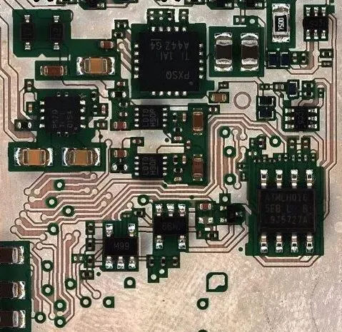
The two key points to keep in mind are: first, the amount of solder allocated on the solder pad should be kept within a controlled area. Solder cannot flow onto the wiring. Figure 1 shows a clean wiring without any solder.

Figure 1: The amount of solder allocated on the pad needs to be kept within the pad
Secondly, it is important to use the minimum amount of solder and allocate only enough to produce high-quality solder joints. As mentioned above, any excess solder will interfere with the performance of the RF circuit.
Determine the correct template
In many cases, EMS suppliers and their assembly personnel do not collaborate with design engineers when designing assembly processes. However, for RF PCBs, circuit board designers play a crucial role in determining the correct template for a given RF circuit board component and must consider certain very important aspects.
For example, he or she must clearly define the device packaging on the critical RF path. During template design, careful consideration must be given to the aperture size of all components on the critical RF path, especially for packages such as flip chip, BGA, and QFN. Any lower or higher solder volume may affect the output performance of the RF board.
The pad design of certain chip types is also crucial. At this point, you need sufficient amount of solder to achieve good solder joints. But in the presence of radio frequency interference, the amount of solder cannot exceed the requirement.
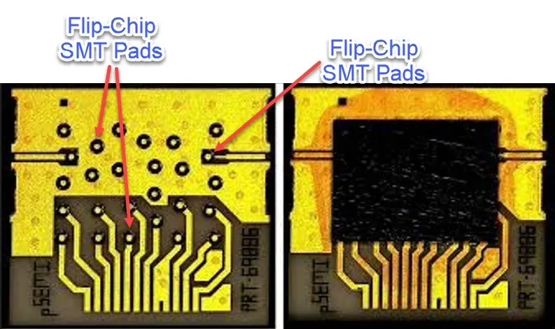
In addition, considering the above points, you must also take into account that newer RF circuit chip installations require increasingly smaller apertures. For example, flip chips are becoming increasingly common in RF circuits, as shown in Figure 2, where they have the smallest solder bumps when connected to the circuit board, resulting in less allocated solder.

Figure 2: The flip chip has the smallest solder bump at the circuit board connection
Solder paste solvent
The complementary circuits of advanced RF chips often use extremely small 01005 size capacitors. The amount of solder allocated on the small solder pads of 01005 solder pads or flip chip active components is a unique challenge, as RF circuits must keep the amount of solder to a minimum while ensuring good fluidity of the solder joints.
As the aperture decreases, the amount of soldering flux required for good flow also decreases. Special attention must be paid to the reflow curve to reduce the amount of flux used and achieve good flow. Solder paste includes soldering flux, which contains solvents, resins, and surfactants required for good flow of solder joints.
Any additional amount of solder on passive components of size 01005 may create thin wire bridging underneath the components. It is worth noting that most X-ray devices (including high-resolution 5DX systems) are capable of detecting bridges beneath resistors, but cannot detect bridges beneath capacitors (especially capacitors of size 01005).
Therefore, assembly plants must have sufficient experience to successfully install a large number of 01005 capacitors on RF circuits and avoid potential bridging. What needs to be repeated here is that the challenge is to have enough solder to achieve good flow, but not too much solder to avoid bridging when placing components.
Grounding hole
Another key aspect of RF performance is good grounding. Grounding is an important aspect of high-speed RF circuits, as current needs to flow through the ground wire to complete the circuit. In QFN type components, the bottom of the chip is a large grounding area.
When refluxing a large area of land, voids of different sizes and percentages will be formed. Voids are gas trapped in solder joints. Reducing voids is challenging, but not impossible. Through careful process design, analysis, and appropriate template design, grounding voids can be reduced to less than 10%.
Reflow profile
Once the circuit board is assembled, the reflow curve becomes crucial. It must consider the volume of solder and available flux to achieve appropriate flow.
Once the solder is printed, the reflow time or the time required to reflow the circuit board becomes crucial.
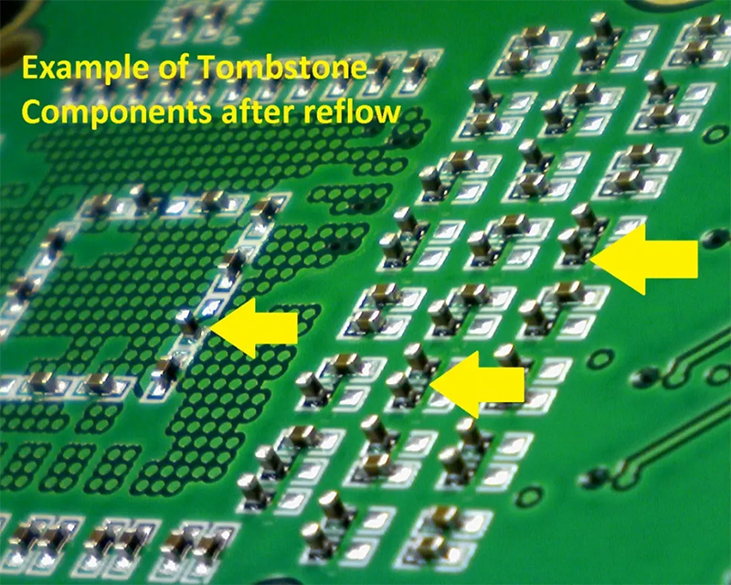
If the time is too long, some solvents in the solder paste on the strictly controlled small solder pads may even evaporate before reaching the reflow system. In addition, once the circuit board begins to reflow, there may be some issues such as dry soldering or standing of smaller passive components or 01005 size components (Figure 3).

Figure 3: The assembly plant must have extensive experience to successfully install passive components, including 01005 capacitors, on RF circuits to prevent monument and bridging
Due to the limited amount of solder allowed for distribution on high-frequency RF circuits, these two challenges have become even more severe. All of these require experience, appropriate equipment, correct tool design, and process control.
Various reflux techniques can be used. This includes carefully controlled conventional convection reflux curves. The gas-phase reflux system is very useful, especially for mixing high-density components and very small components on the same side. The vacuum vapor phase system is also crucial for reducing voids, and in some aspects, reflow becomes even more critical considering the volume of solder and the available solvent in the solder paste.
functional testing
OEM provides information or specifications for functional testing to assembly plants. Due to frequency and test point creation limitations, custom functional testing on RF type circuits is sometimes the only available testing method. Testing points are not common on RF circuits, therefore, without testing points, both flying pin testing and online testing are inefficient.
Therefore, the functional testing of RF circuits can be performed using devices such as Vector Network Analyzer (VNA) for waveform analysis. This level of advanced functional testing requires experienced engineers, technicians, and programmers.
But it must be pointed out that functional testing has its own limitations, as it cannot tell you the details of the fault, which is why the process of RF components must be extremely strict from beginning to end. You don't want the functional tester to take responsibility for fault detection because it cannot accurately locate these faults.
summary
As we mentioned here, RF PCB belongs to the category of complex components. But its uniqueness lies in the need for experienced assembly workshop engineers and technicians to plan and execute key aspects such as component selection, PCB materials, correct template design, attention to complementary circuits, reflow curves, and functional testing.
Most importantly, the template must be almost flawless to prevent excess solder from being distributed onto the circuit board. Therefore, OEMs looking for RF PCB assembly plants should consider evaluating their requirements based on the above assembly steps.