PCB wiring has inductance and capacitance, which together determine the impedance of the wiring.
Sometimes, understanding the inductance of the wiring can help estimate the coupling caused by crosstalk.
Although there is no specific wiring inductance value set, it is a powerful tool for understanding signal behavior in certain systems.
All PCB wiring has a certain inductance, but do you know how the inductance in PCB wiring affects electrical behavior? The different conductor systems in PCB require specific routing widths, which will determine the inductance of the routing. However, there is no specific empirical rule for PCB routing inductance, only calculation formulas related to routing impedance can be used to determine routing inductance. In addition, there are no specific regulations requiring us to use specific routing inductors as design goals in circuit board design.
After understanding the important factors that determine the input impedance of wiring, it is easier to determine when to deviate from the impedance target and choose higher or lower wiring impedance in circuit board design.
Empirical rules for PCB wiring inductance
In transmission line design, the calculation of routing width often starts from the selection of stacking design and transmission line geometry structure. Other systems, such as power converters, may not require impedance control along the traces, so they typically use wider copper traces to reduce inductance. When calculating inductance, impedance should be calculated first, and then impedance should be used to calculate the routing inductance.
Impedance calculation formula
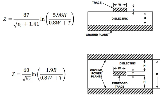
The most basic impedance model used in the PCB industry is the formula in the IPC-2141 standard. The impedance calculation formulas for IPC-2141 microstrip and strip lines shown below are based on experimental observations and have high accuracy in the frequency range below 1GHz.

IPC-2141 microstrip and strip line impedance calculation formula
It has been proven that the above formula is not entirely accurate and contains some assumptions that are not always valid. Specifically, the above formula has the following shortcomings:
Neglecting the loss tangent: All PCB laminates will experience some attenuation, which can be quantified using the loss tangent. The loss tangent usually increases some reactance, causing a slight change in the impedance of the wiring.
Copper roughness: The skin effect and copper roughness have been integrated into the above formula, and they cannot be separated separately without using more complex methods (such as the IEEE model). Therefore, the above formula is not applicable to all manufacturing processes and material systems.
Although the above formulas are not perfect, they provide a good starting point for calculating trace impedance and are applicable to many situations in PCB design.
Calculate inductance based on impedance
After designing the routing width to achieve the impedance target, the routing will have a specific inductance. The design process is generally not reversed unless it involves low-speed digital signals, low-frequency analog signals, or switching power converters with specific low inductance requirements. If the routing length is short enough, it is possible to deviate from the typical 50 ohm impedance target during design and use lower routing inductance.
In summary, there is no empirical rule for PCB routing inductance. In other words, there is no specific requirement for wiring inductance, nor is there a simple formula to calculate the wiring inductance of all PCBs.
To delve deeper, we can refer again to the IPC-2141 calculation formula and the constitutive impedance relationship of lossless transmission lines. The IPC-2141 equation contains a formula for calculating capacitance per unit length, which can be used to calculate PCB routing inductance.

Microstrip and stripline capacitors
In the specific configuration mentioned above, the routing capacitance is defined relative to the nearest ground plane. Finally, we obtained two formulas for calculating the inductance of microstrip lines and strip lines, respectively.

Microstrip and stripline inductors
From this, we can see that the routing inductance depends on:
Wire thickness (or copper weight)
Layer thickness
Geometric structure of wiring
To ensure that the design meets impedance targets and determines inductance, these factors must be considered simultaneously. When calculating inductance, the layer thickness (H or B) and copper weight (T) are usually fixed, and impedance and/or wiring density targets need to be met by determining the wire width. When designing wiring on a stack of specific laminated materials, if the same wiring is placed in a PCB stack made of different dielectric materials, the inductance or impedance will change. If necessary, various stacked inductors and width curves can be compared.
Limitations of PCB wiring inductance rules
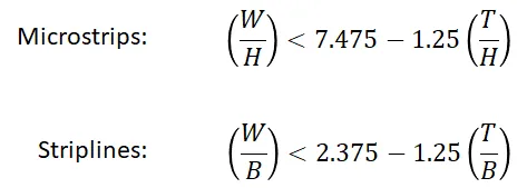
Because the above equation is a logarithmic equation, it is only valid within a certain range of geometric parameters. As long as the parameter in the above logarithm is less than 1, the calculated inductance is negative. By rewriting the parameters in the logarithm as ratios (W/H) or (W/B), as well as (T/H) or (T/B), we obtain the following inequality, which limits the allowed geometric structures of the lines in the above formula:

In order to make the inductance of IPC-2141 non negative, it is necessary to limit the geometric structure of microstrip and strip lines
For example, we can observe microstrip line inductance in a simple PCB stack with impedance control. On a four layer circuit board using 0.5 ounce/square foot copper traces (dielectric thickness 8mil, Dk=4.2), the required trace width to achieve a 50Ohm impedance is 15.15mil, and the inductance is 6.679nH/inch. The results obtained by other models are vastly different, which is sufficient to indicate the shortcomings of IPC-2141.
In addition to using the outdated IPC-2141 formula, there are better methods to determine the impedance and inductance of the wiring. More effective PCB stacking and routing calculators include moment method field solvers or boundary element method field solvers. These tools can be used to quickly calculate the PCB routing inductance on a circuit board with a given stack and impedance target, and then use this inductance value to determine rough crosstalk results. Some highly sensitive precision measurement designs or power converters require extremely low inductance wiring, and these calculations can be used as references for verification.
Cadence's PCB design and analysis software can be used to validate any PCB routing inductance empirical rules when evaluating advanced electronic designs. Designers can use powerful field solvers and circuit modeling tools to simulate electrical behavior and calculate many important signal integrity indicators. When using Cadence's software suite, we can also access a range of simulation functions that can be used for signal integrity analysis to comprehensively evaluate system functionality.